Ionic-Liquid Gating of MoS2
![]()
University of Regensburg
Institute for Experimental and Applied Physics
March 19, 2024
Motivation
MoS2 excellent 2D semiconductor

- Strong spin-orbit coupling
- Spin split bands
- Broken inversion symmetry
\(\Rightarrow\) Quantum Dots (Schock et al. 2023)
Intrinsic superconductivity (SC) in flakes
- Induced via liquid-ion gating (Zhang et al. 2012; Taniguchi et al. 2012)
- SC in single and multi layer MoS2 (Costanzo et al. 2016)
Also: Thickness dependend SC in WS2 nanotubes (NT) (Qin et al. 2018)
Objective:
- Find good fabrication and measurement methods using MoS2 flakes.
- Apply findings to MoS2 nanotubes.
- Achieve SC in MoS2 nanotubes.
MoS2 Nanotubes
- Grown via chemical transport reaction by group of Prof. Dr. Maja Remškar (Ljubliana)
- Nanotubes and -ribbons
- Thickness from several hundred nanometers down to 20 nm
- Length up to mm scale

Liquid-Ion Gating
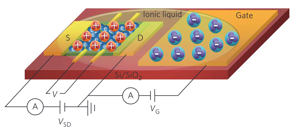
(from Costanzo et al. 2016)
Liquid-Ion Gating

- ALiquid-Gate > ADevice
- Apply voltage to liquid-gate
\(\rightarrow\) Ions deposit on device and create large capacitance
\(\rightarrow\) Increase of surface carrier density (n ~ 1014cm-2 (Zhang et al. 2012))
\(\Rightarrow\) Metallic transport in the MoS2 channel
\(\Rightarrow\) Transition to superconductivity for 1.5 K < T < 10 K
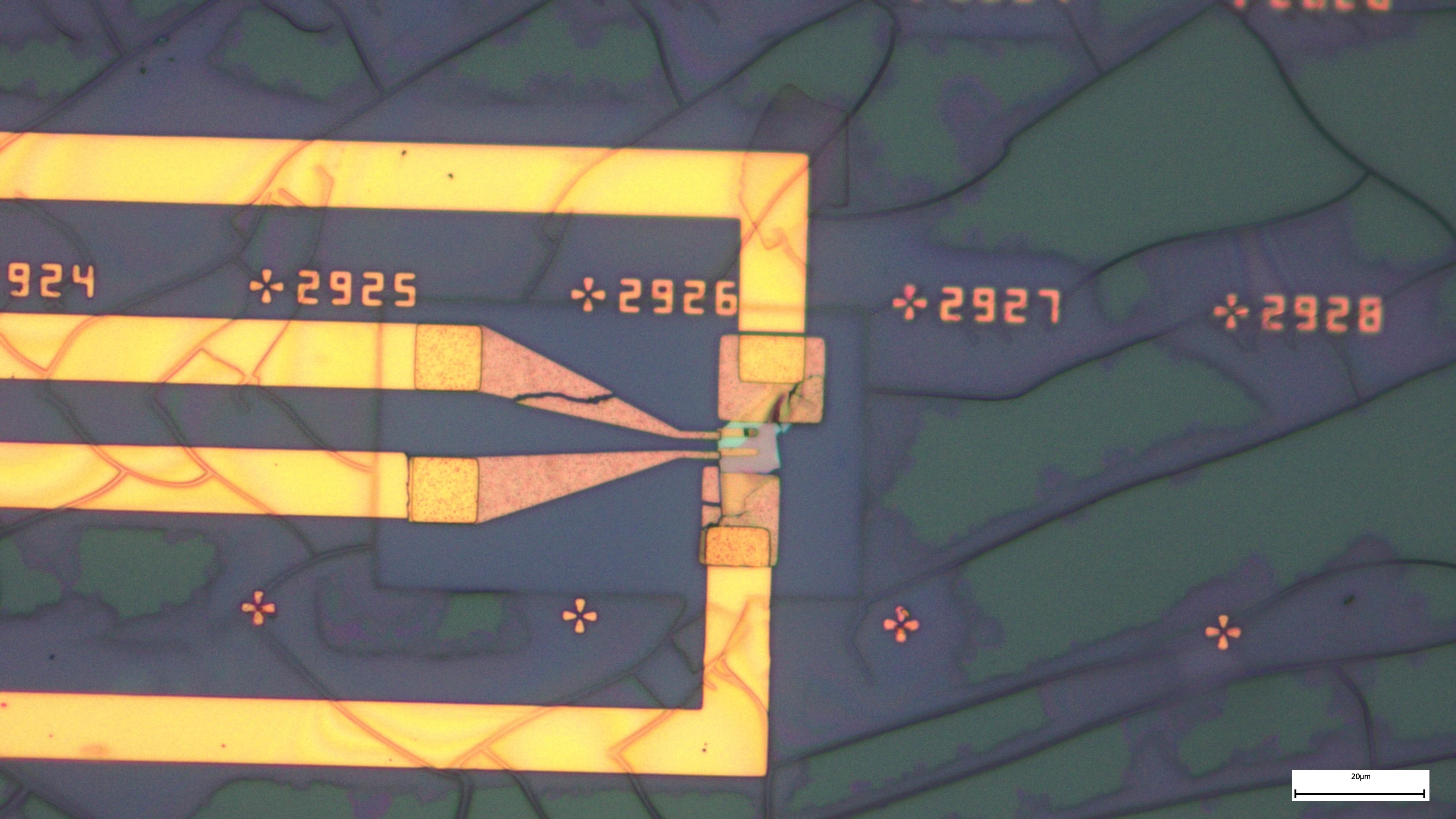
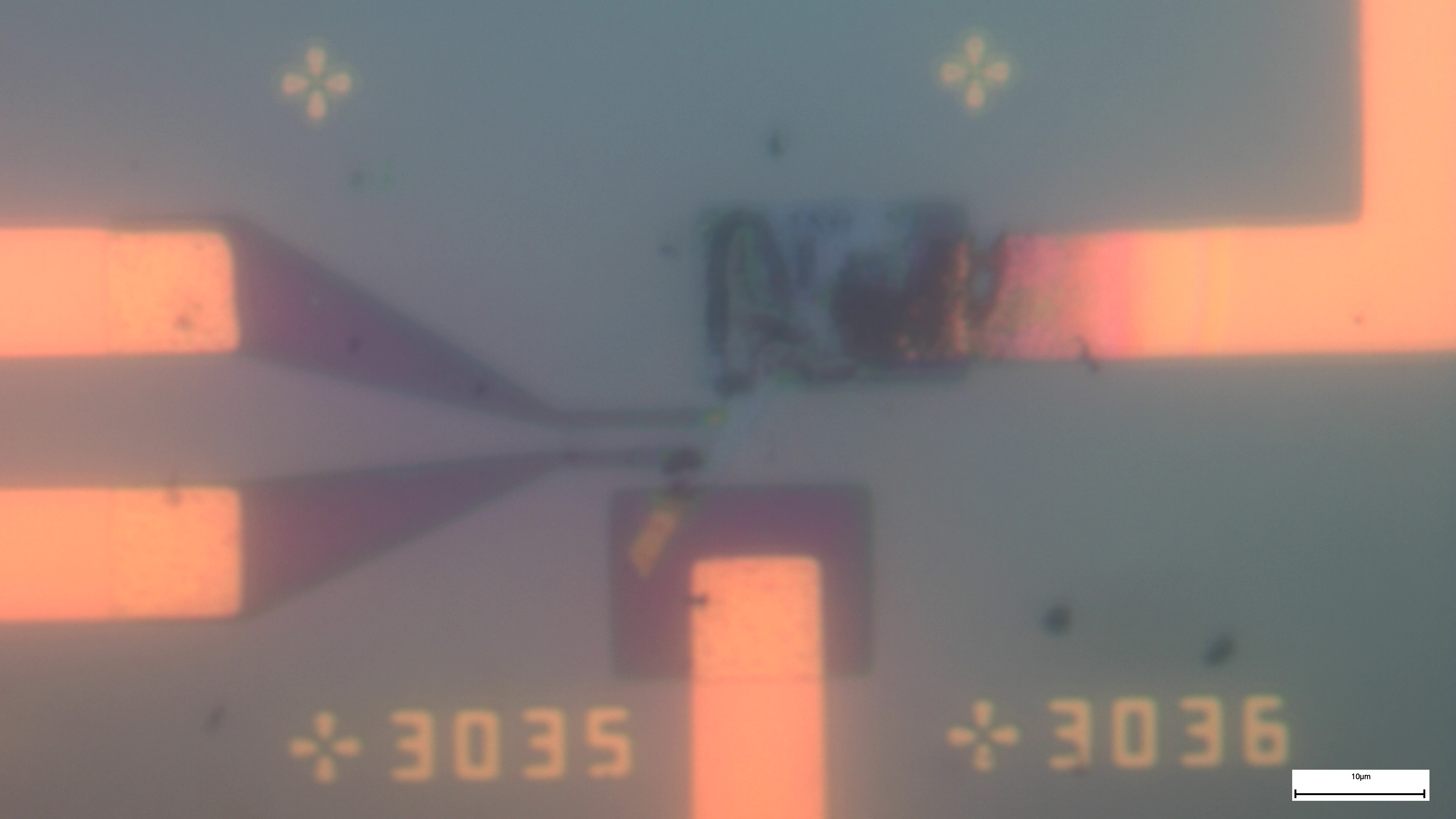
Device Preparation

- Transfer MoS2 via Blue Nitto Tape onto Si/SiO2
- Fabricate Bi/Au contacts with standard lithographic methods
- Apply protective resist layer with windows over MoS2 sample
- Add drop of DEME-TFSI
Design

Design
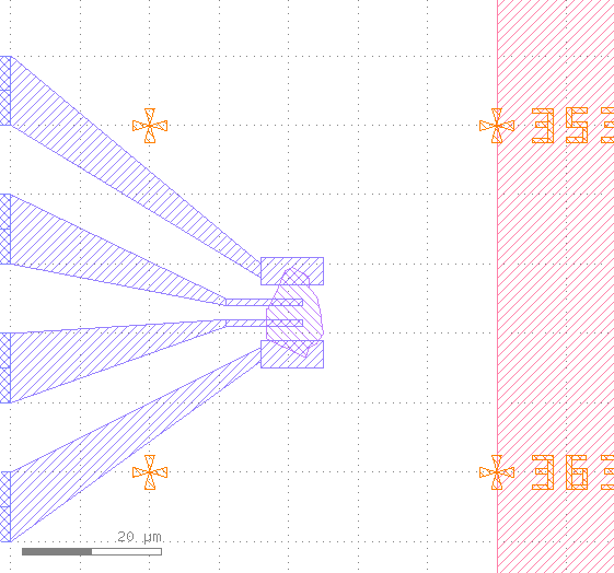
Finished Device

Interlude: Why Bismuth?
- Bismuth allows for Ohmic contacts to MoS2 (Shen et al. 2021)

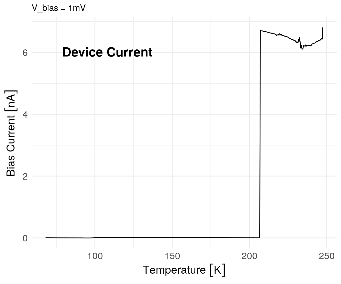
Liquid-Gate Sweep
Two Main Problems Arise
Device “Cracks” during Cooldown
Device Degradation
Two Main Problems Arise
Device “Cracks” during Cooldown
- DEME freeze out leads to shear forces
- Bi/Au contacts break
\(\rightarrow\) Cr/Au or Ti/Au contacts
Device Degradation

Two Main Problems Arise
Device “Cracks” during Cooldown
- DEME freeze out leads to shear forces
- Bi/Au contacts break
\(\rightarrow\) Cr/Au or Ti/Au contacts
Device Degradation

Two Main Problems Arise
Device “Cracks” during Cooldown
- DEME freeze out leads to shear forces
- Bi/Au contacts break
\(\rightarrow\) Cr/Au or Ti/Au contacts
Device Degradation
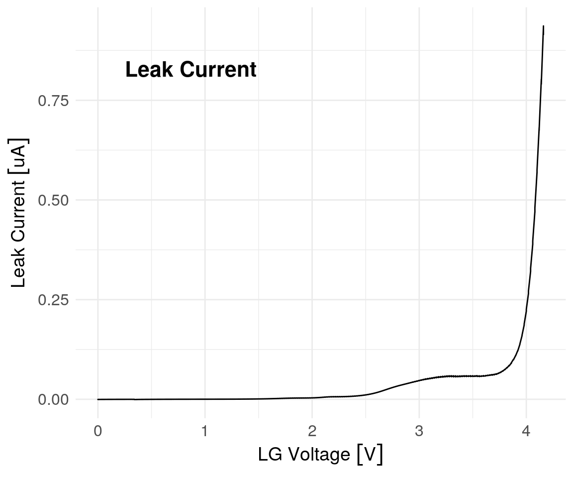
- Leakage current indicates device degradation
- Decreases with decreasing Temperature
\(\rightarrow\) Keep Ileak < 1nA, T \(\le\) 220K and VLG <= 3V
Suspend Nanotubes (1): Double Resist

- MoS2 NT wedged between to layers of resist
- Au contacts deposited around NT
- Protective resist and a drop of DEME-TFSI
Suspend Nanotubes (2): Anthracene Transfer

- Anthracene crystals are grown in our clean-room
- MoS2 NT is picked up using an anthracene crystal stuck to PDMS and placed onto contacts
- Anthracene is evaporated at 130 °C
\(\rightarrow\) Dry and very clean transfer
- A drop of DEME-TFSI is applied
Acknowledgments
- PD. Dr. Andreas K. Hüttel
- Robin T. K. Schock
- Prof. Dr. Maja Remškar
- Prof. Alberto Morpurgo for his advice

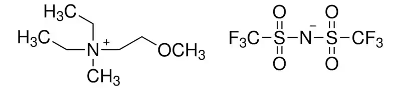
“DEME-TFSI is short for?”
![]()